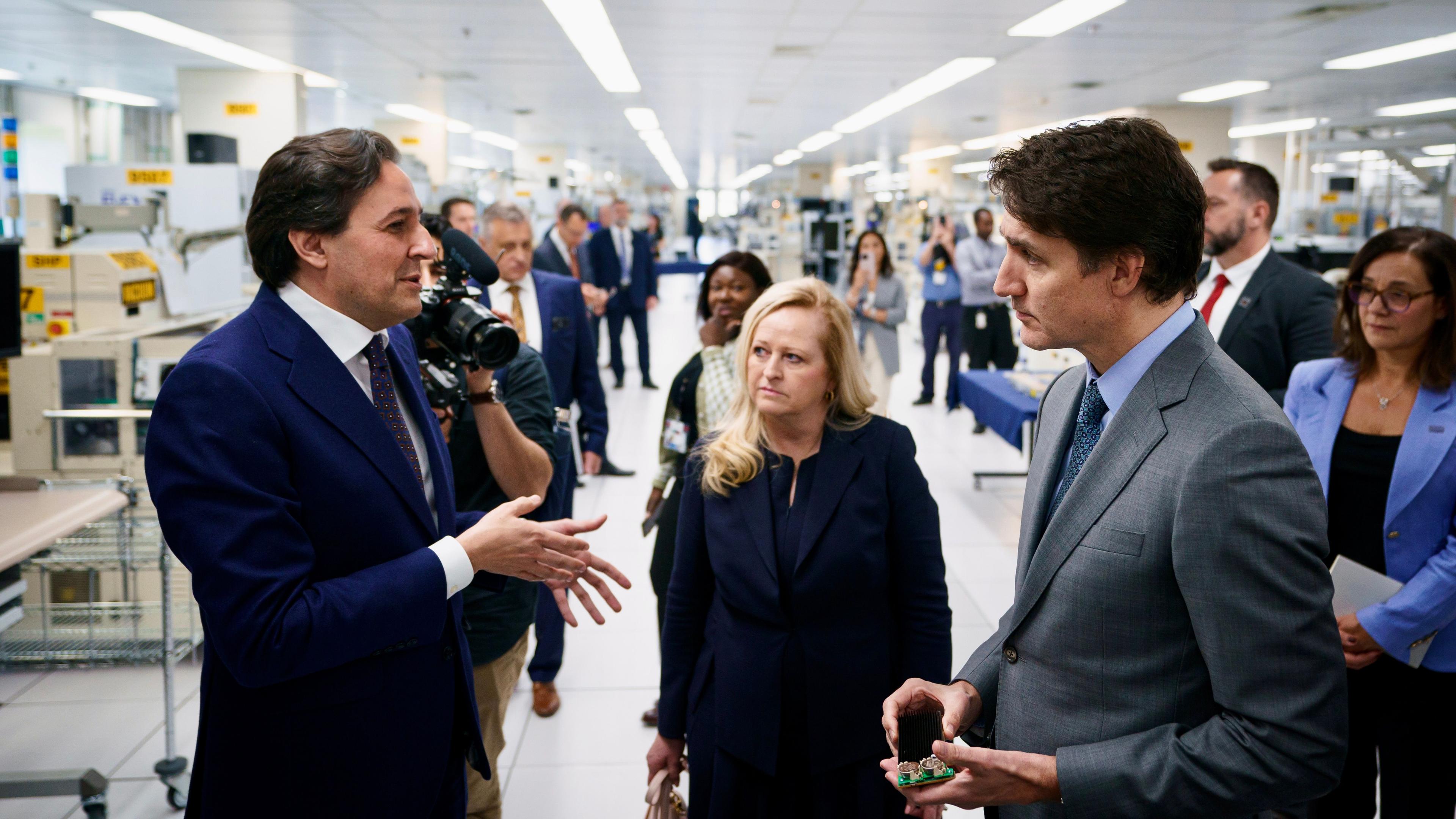
Silicon Nanophotonic Packaging - Photonic Flip-Chip
Concept
The core advantage of silicon photonics is large scale integration of devices on a single chip resulting in low-cost photonic circuits of high complexity. However, it is not always possible or practical to integrate all desired photonic materials on a silicon chip. Integrating a given material on silicon may not be manufacturable or the performance, cost, or reliability penalty related to such integration may be too large to be practical. Hence, a solution to cost-efficient assembly of multiple optically and electrically interconnected photonic chips is key to broad enablement of integrated photonic technology.
We employ solder self-aligned photonic flip-chip assembly for integration of optically, electrically, and thermally interconnected photonic chips. The assembly process is illustrated below. A secondary photonic die, including III-V or non-linear optical materials, is picked and placed into a shallow recess on the Si surface. The metal pads on the Si and the secondary die are purposefully offset by design. At solder anneal, the surface tension of the solder will exert a substantial force towards re-centering of the metal pads to minimize the solder surface area. The resulting chip movement can be stopped with precisely defined mechanical alignment stops for accurate self-alignment at anneal. Optical connections between the Si photonic circuit and the secondary die are performed with butt-coupling while thermal and electrical connections reuse the flip-chip solder pads employed for re-alignment. This assembly process can be performed at Si wafer level or on individual Si chips.
The notion of applying solder surface tension to re-alignment is not new and has been around in the research domain since the 70’s. What is different here is the dimensional scale on which this is done and the sought final alignment yield and accuracy.
Butt-coupling was chosen for optical chip-to-chip connections for universality amongst material systems. Other approaches, such as adiabatic or diffractive coupling, can be more forgiving to chip misalignment but require an effective-index crossing and high index-contrast interfaces, respectively. This limits the usability of such approaches across disparate material systems.
The key challenge in chip-to-chip butt coupling connections is alignment accuracy. As shown below, the optical connection must be done at maximum mode delocalization to maximize alignment tolerances. However, even with substantial mode engineering, the largest mode that can be practically achieved across material systems is inherently smaller than a fiber mode so the self-alignment needs to be more accurate here than in a fiber connection. To achieve this, we employ lithographically defined mechanical stops on both the secondary die and the Si photonic circuit. Tolerance analysis indicates that sub-micron self-alignment accuracy is achievable if the mechanical stops are carefully designed on adequate lithographic layers.
The field profile of the Si waveguide coupler employed here is shown above on the right. It resembles a strip-loaded waveguide. The vertical confinement is provided by common CMOS middle-of-the-line planar layers while the lateral confinement is provided by a nanotaper coupler or a metamaterial coupler on a silicon-on-insulator layer. A metamaterial is an engineered material with sufficiently fine patterning to appear to the optical waves as a homogeneous material with engineered properties. Such elongated mode is well suited to the realities of chip assembly where the vertical alignment accuracy is generally better than the in-plane alignment accuracy. In addition, it can be universally achieved across material systems. For instance, we find better than 95% mode overlap between the metamaterial coupler shown above and a typical rectangular multimode InP waveguide.
Implementation
Our first demonstration of three-dimensional solder-induced self-alignment was performed with a secondary photonic die made of Si. A first generation design is shown below.
The receiving structure on the primary die is shown on the left and the secondary die is shown on the right. A recess in the primary die is required for the needed clearance to lower the buried waveguide on the secondary die to the height of the buried waveguide on the primary die. Standoffs in the recess are used as vertical mechanical stops for precise vertical self-alignment. A ridge on the secondary die acts as the lateral mechanical stop for precise self-alignment in the direction transversal to the waveguides. During re-alignment, it butts on a standoff defined in the primary dies’ recess. In the longitudinal direction, along the coupling waveguides, the re-alignment movement is stopped by butting of the dies’ optical coupling facets.
Demonstration
The micrographs below show assemblies after self-alignment. A cross-section of a laser lateral stop butted on a Si standoff is shown on the left. A perspective view of a secondary die assembled to a photonic chip is shown on the right. These first generation results were presented at ECTC 2015. The manuscript is available in pdf format here.
Once butting of mechanical stops is achieved, the alignment accuracy is limited by the patterning accuracy of the mechanical stops. This includes lithographic alignment accuracy and etch dimensional control. The patterning accuracy, and thus alignment accuracy, will depend on the stops design and the fabrication tools used.
Our first optical demonstration of solder self-aligned photonic flip-chip was reported at FiO 2016. The conference proceedings are available in pdf format here. The experimental setup and the corresponding spectral response is shown below. Waveguide loopbacks on the secondary die connected pairs of waveguide couplers on the primary die. The chip-to-chip loss was established by probing the primary die with lensed fibers and calibrating out the fiber-to-chip and the on-chip propagation loss with a reference waveguide. The Fabry-Perot oscillation from the lensed fiber connections to the primary die was filtered out and the resulting curve super-imposed in blue over the raw data drawn in grey. A peak transmission of 1.1 dB with a very flat spectral response was obtained. This optical performance confirms sub-micron waveguide-to-waveguide alignment accuracy.
Yield and manufacturability
As mentioned above, the notion of applying solder surface tension to flip-chip re-alignment is not new and has been around in the research domain since the 70’s. However, we have not seen reports of solder surface tension re-alignment being used in large-scale manufacturing. This suggests that there might be an unspoken issue with such approach preventing the transfer from research to production. We have identified such a manufacturing obstacle in the form of a sharp yield concern in our first experiments. Some samples would re-align properly while others would not complete their re-alignment movement or not move in a meaningful way. We have explored a significant number of potential yield affecting mechanisms and found that sensitivity to solder volume in the re-alignment pads created a sharp yield limit. This was confirmed with computational studies and meso-scale experiments.
The uniqueness of our most recent designs originates from us finding a design-based solution to this sensitivity to solder volume. Our approach is based on creating solder reservoirs that can self-correct the solder volume in the re-alignment pads. This approach was first patented and was then published at ECTC 2016. The manuscript is available in pdf format here. The computationally obtained sensitivity to solder volume is shown below for a typical design and a novel design including solder reservoirs. Adequate re-alignment will be favored if the in-plane solder force is larger than the vertical solder force. We find the fabrication window on the solder volume to expend from 6% on a typical design to almost a factor 2 in our novel approach. A typical tolerance on solder plating is of about +/- 10%. Considering additional fabrication tolerances we find that a tolerance on solder volume of +/- 15-20% would be desired for high-volume manufacturing. We currently expect to exceed such tolerance.
Our goal is the broad enablement of low-cost silicon photonic packaging. Please contact us if you would like to make use of any of the described technology.
Tymon Barwicz et al.
Related Projects
More Information
- Project Overview from 2016 (JSTQE 2016 overview paper, PDF)
- Project Overview from 2015 (Group IV Photonics 2015 plenary talk, slides in PDF)
- Parallelized fiber assembly results (Proceedings of ECTC 2015. PDF)
- Compliant interface optical performance (Proceedings of FiO 2016. PDF)
- Compliant interface self-alignment (Slides from Barwicz et al., ECTC 2014. PDF)
- Solder-aligned photonic flip-chip optical perfromance (Proceedings of FiO 2016. PDF)
- Solder-induced self-alignment yield (Proceedings of ECTC 2016. PDF)